Business Portfolio
Semiconductor and electronic component material specialist
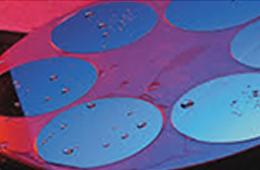
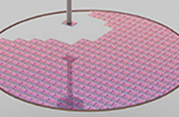
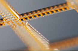
Semiconductor
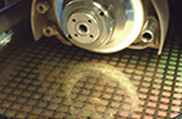
Lead frame surface treatment
Purpose
Electronic component SMT soldering improvement
Lifetime improvement by antioxidation
Eco-friendly surface treatment
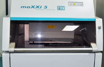
Process
Electro Deflash
Water Jet
Descale
Electro Plating
Post treatment
LED process flow
Purpose
Deflash
Process
Electro Deflash
Water Jet
Descale
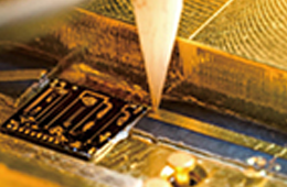
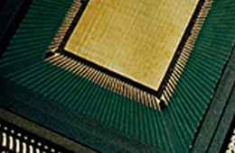
Assembly
Process
FAB
ASS’Y
Back Grinding
Wafer backgrinding
Sawing
Wafer saw
Die Attach
Chip attach on lead frame
Wire Bond
Wire bonding
Molding
Molding
Metal Finish
Prevention of lead frame oxidation
Conductivity and solderability improvement
Trim / Form
Trim / Form
TEST
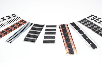
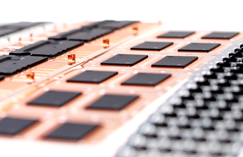
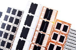
| Package | Electro Plating | |||
|---|---|---|---|---|
| Composition | Thickness | Length | Width | |
|
TSOP(I,II), QFP, SOIC, PLCC, DIP Power Module LED Sensor |
Pure Tin Tin Bismuth Au Plating |
4~25 ㎛ |
150~250 ㎜ |
30~75 ㎜ |